
When a photovoltaic module is partially shaded there is a risk of hot spots known as hot spots.
The solar panel contains a mechanism that aims to reduce the negative impact that a partial shading may cause in the module. To do this, a bypass diode, also known as a bypass diode, is used. bypass.
In this article, the equivalent circuit of a module and its energy generation principle will be shown, in order to explain how the hot spot and what is the role of the diode? bypass.
Characterization of a diode
The diode is an electronic component whose operation is similar to that of a valve – the device allows the passage of electric current in only one direction and blocks the passage in the opposite direction.
The PN junction diode conducts current when there is a voltage between its positive and negative terminals greater than a certain threshold value, typically 0.7 V for crystalline silicon diodes.
This voltage is called forward bias voltage. In forward polarization, the diode behaves as a good conductor above a voltage of 0.7 V.
As long as the polarization voltage is not reached or if the device is reverse polarized across its terminals, the diode does not conduct current.
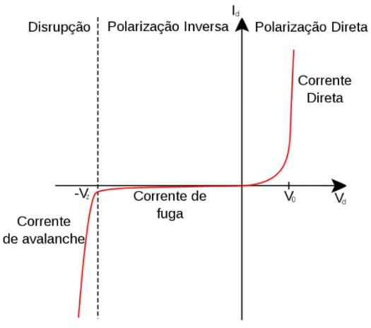
When the diode's reverse polarization exceeds the diode's breakdown voltage, it loses its ability to block current in the reverse direction, potentially damaging itself in the process and allowing a high current to pass, called avalanche current. The typical operating curve of a diode is shown below.
Characterization of photovoltaic cells
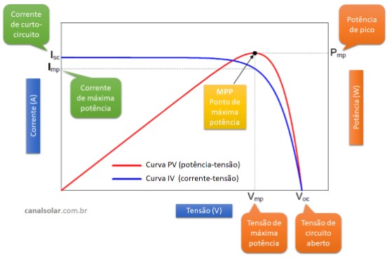
Photovoltaic cells have a structure similar to that of a PN junction diode, with the difference of being capable of generating electricity through the photovoltaic effect. The photovoltaic effect explains the generation of voltage and current in a semiconductor material exposed to light. In short, photons of light interact with electrons in the valence shell of semiconductors and cause the appearance of a current, which is proportional to the number of interactions between photons and electrons in the crystalline structure. This current flow in a PN semiconductor causes an internal voltage to appear in the material. When this internal voltage reaches a certain limit, part of the current generated by the photovoltaic effect is diverted through the cell's PN junction, limiting the amount of current that can be supplied to the circuit. The sum of these two phenomena — the generation of current by the photovoltaic effect and the diversion of part of this current through the PN junction — results in the cell's I x V characteristic curve. To learn more about the module's I x V curve, read our article: Understanding the IV and PV curves of photovoltaic modules.

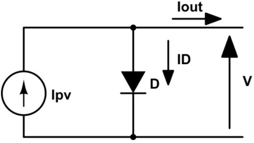
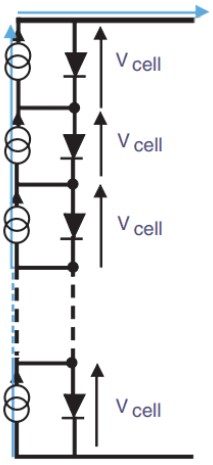
We can model an ideal photovoltaic cell using the circuit below (Figure 4), where the current source characterizes the photovoltaic effect and depends only on the quantity of photons of light that fall on the semiconductor, while the diode characterizes the nature of the cell's PN junction.


It is called generation current (IPV) to the current generated by the photovoltaic effect and dark current (Id) the current diverted by the internal PN junction.
To characterize a photovoltaic module composed of ideal cells, we must connect the equivalent circuits of each cell in series, as shown in Figure 5 below.
Causes and prevention of hot spots
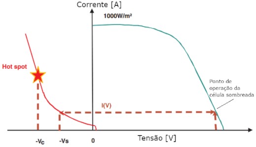
When the module is operating without shading, the generation current of each cell is equal, and the voltage at which the diode representing the PN junction is located is such that there is only a small flow of dark current through it. When a cell is shaded, the source that represents the photovoltaic effect ceases, meaning that the only path for the current generated by other cells is the PN junction of the affected cell. The voltage to which the PN junction of the affected cell is subjected causes the equivalent diode to operate in the reverse bias region, allowing the circulation of a current equal to the generation current of the other cells, but dissipating a large amount of energy. The power dissipated in the reverse-polarized junction (or cell) is equivalent to the product of the generation current of the other cells and the negative reverse voltage. PFor a typical arrangement of modules, 20 cells of 0.5 V each and 9 A of generation current, the power dissipated would be in the order of 80 W, enough to damage the shaded cell and cause a localized temperature increase, known as hot spot.
To avoid the emergence of a hot spot There must be a mechanism that when one or more cells in a series are shaded, there is a path of least resistance for current from the other cells or series to flow.
The device that diverts the current and prevents hot spot is the diode bypass. When the cell or module is operating without partial shading, the bypass It is reverse biased and does not conduct current.
When shading occurs, it is sufficient to activate the diode. bypass, current is diverted from the affected circuit.
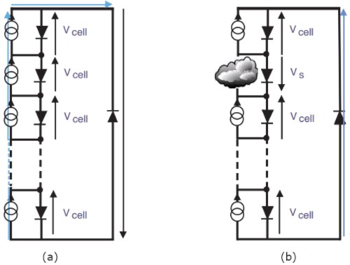
Activation of the diode bypass causes the current from the affected series to circulate only in the series itself, and cannot be exported to the rest of the circuit. This causes a drop in production of the affected module.
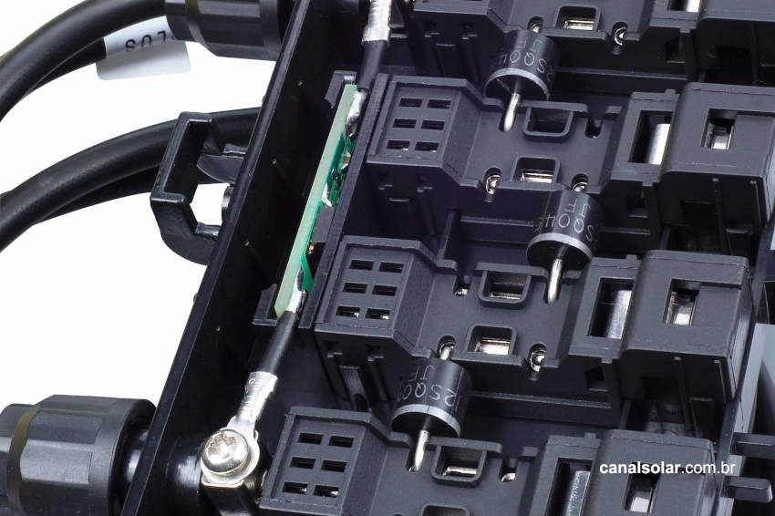
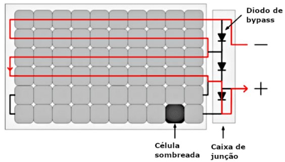
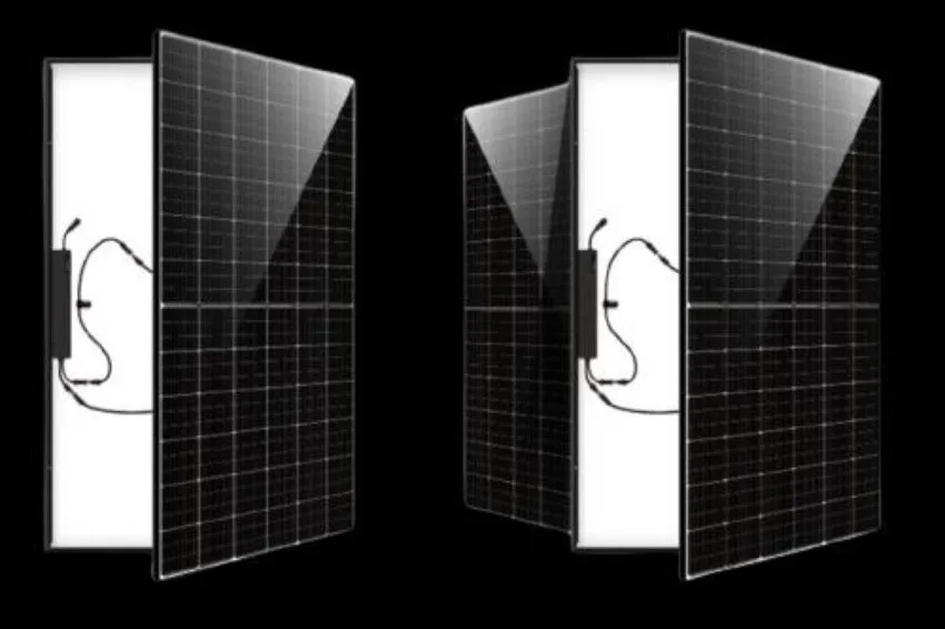
PTo prevent small shadows from causing a module's total output to drop, manufacturers arrange the module's array of cells in such a way that there are typically 3 diodes. bypass, which are allocated in the junction box.
In this way, a shadow on a cell diverts the current of only ⅓ of the affected module from the circuit.
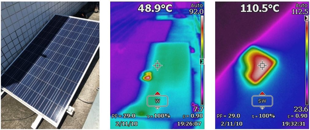
Since shading is the cause of the appearance of hot spots and the activation of the diode bypass, this must be avoided during the system design stage and in the field by cleaning any animal waste or dirt.


One Response
Dear Matthew,
I enjoyed reading your article regarding shading and hotspot and I would like to
talk to you about this matter, if I can call or send
an e-mail.
Thank you very much in advance.
Att.
José R Bueno