Currently, N-type photovoltaic cells are winning the solar energy market.
Maybe you don't know or have never worried about it, but the cells used in the manufacture of photovoltaic modules have always been type P. Why this change now?
N-type photovoltaic cells are more efficient, but the market has always preferred P-type cells, both monocrystalline and polycrystalline.
Initially, P-type silicon was preferred and its manufacturing developed more rapidly because of its high tolerance to damage from cosmic radiation, which made it ideal for aerospace applications.
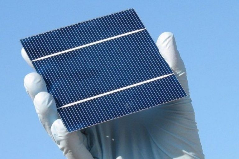
What differs between P and N silicon is the doping process in the manufacture of the ingot with which the wafers are manufactured. Wafers are silicon wafers that will later be transformed into photovoltaic cells. Traditional cells are manufactured using P-type wafers, while N-type cells are manufactured using N-type silicon wafers.


After wafer manufacturing, the next step in cell manufacturing is final doping. In type P cells, the final doping adds an N layer on the P wafer, forming the PN junction, as seen in Figure 2. On the other hand, in the type N cell, the N wafer is finally doped to receive a silicon layer from the type P, as we see in the same figure.
P-type cells dominated the market because in the early years of the production of photovoltaic materials, most of this demand came from space agencies for the production of satellites and other equipment that helped in space exploration, since P-type Si is more resistant to degradation caused by exposure to cosmic rays.
Faced with this demand, industries began producing P-type solar cells and have continued to do so to this day. However, P-silicon also has other advantages, such as the lower temperatures required for phosphor diffusions to form the PN junction compared to the boron diffusions required for N-type cells, along with the fact that the diffusions of phosphorus allow the effective removal of metallic impurities from polycrystalline silicon.
In other words, manufacturing P-type cells uses less energy and is simpler. Although the first silicon solar cell developed by Bell Laboratories in 1954 was N-type, P-type cells predominated in the industry market.
The advantages of P-type silicon led to its initial market dominance and resulted in the technology being preferred by equipment suppliers and industrial process development.
However, more recently the search for more efficient photovoltaic modules has turned the market's attention to N-type silicon, which from an application point of view, despite more complex manufacturing, has significant advantages over P-type silicon.
The most important characteristic of N-type silicon is the longer carrier lifetime (free electrons), caused mainly by the absence of the well-known boron-oxygen feat. The useful life of the carriers is directly related to the efficiency of a photovoltaic cell.
This is the fundamental reason behind the fact that the highest efficiency modules available on the market today employ N-type cells. N-type silicon's market share is still small. Despite its greater efficiency, its cost is higher.
Many companies and research centers are now working on developing N-type solar cells, trying to reduce their production cost while seeking higher efficiencies.

The boron-oxygen effect
The evolution of solar cell technology has occupied a significant space in the photovoltaic market. The vast majority of solar cells are crystalline silicon (Si) wafers that are responsible for converting light energy into electrical energy.
They can be made of monocrystalline silicon (mono-Si), polycrystalline silicon (multi-Si) or amorphous silicon (a-Si). The set of these photovoltaic cells forms solar modules. As we know, what differs between P and N silicon is the doping process in the manufacture of the ingot. P silicon is doped with boron and N silicon is doped with phosphorus.
During the crystalline ingot formation process, oxygen penetrates the silicon. This problem is about three times more intense in monocrystalline silicon, manufactured using the Czocralsky method, than in polycrystalline silicon.
The big problem is that the oxygen present in silicon joins with boron to form carrier recombination centers, which reduce the lifetime of electrons available for the formation of electric current. In other words, the presence of the boron-oxygen complex makes crystalline cells less efficient.
So, the main cause of the low efficiency of P-type cells, which have always been the market's favorite, is the so-called boron-oxygen effect. N-type silicon does not suffer from this. Therefore, with it we can manufacture more efficient cells. The formation of the boron-oxygen complex occurs within the first hours or weeks of exposure of the cell to light.
This is the main cause of the well-known LID (light induced degradation) effect, which reduces the efficiency of photovoltaic cells by 2 to 4%. N-type silicon, on the other hand, does not suffer from this problem.
Difficulties in manufacturing N-type silicon
In addition to using more energy, as we mentioned at the beginning of the text, the manufacture of N-type monocrystalline silicon presents a difficulty in relation to the ingot growth process. In the manufacture of type P ingots, the boron dopant has a more homogeneous distribution of concentration.
This means that the amount of boron remains approximately constant throughout the length of the ingot and there is little difference in concentration from one end to the other. Speaking in simple language, cells manufactured from P-type ingot have approximately the same characteristics regardless of the part of the ingot from which the wafers are extracted.
In the case of N-type silicon, on the other hand, the scattering of the phosphorus dopant is not so homogeneous. This results in ingots with a large difference in dopant concentration between one end and the other. In short, only one end of the ingot allows you to obtain high-efficiency cells, while cells at the other end will be less efficient.
This leads to low ingot utilization and naturally increases the production cost of N-type monocrystalline silicon. Another problem associated with N-silicon is the difficulty in passivating the cell. Passivation is a technique that has been widely used in modern PERC (passivated emitter rear contact) cells.
Basically, passivated cells are those that have a thin layer of some other material glued to the silicon layer. This improves the electrical and optical properties of the cell, making it more efficient. The industry finds it easier to passivate P silicon than N silicon, which is yet another obstacle in expanding production and reducing the cost of this type of silicon on the market.
Conclusion
Much has been made of solar modules made with N-type cells. Manufacturers are using this cell because of its additional benefits, such as the potential to achieve high efficiency.
Because they use phosphorus instead of boron, they are immune to boron-oxygen defects that cause lower efficiency in PA cells. The N cell is more efficient, but its manufacturing is more complex. The P-type cell has always been the most used on the market, since the beginning of the popularization of photovoltaic solar energy until today.
The biggest concern in the market, which makes it difficult to fully adopt N-silicon in place of P-silicon, is the development of a low-cost technology for processing N-type cells. Several international manufacturers are involved in research and development to reduce the cost and increase results.
References
- The emergence of n-type silicon for solar cell manufacturing, Daniel Macdonald, Australian National University, Canberra
- Advancements in n-Type Base Crystalline Silicon Solar Cells and Their Emergence in the Photovoltaic Industry, Atteq ur Rehman and Soo Hong Lee, Green Strategic Energy Research Institute, Department of Electronic Engineering, Sejong University, Korea
- N-type solar cells: advantages, issues, and current scenarios, Bandana Singha and Chetan S Solanki, Department of Energy Science and Engineering, Indian Institute of Technology Bombay, Mumbai, India
- https://www.cedgreentech.com/article/solar-cell-efficiency-n-type-v-p-type
- https://www.cleanenergyreviews.info/blog/solar-pv-cell-construction