
German research institutions and companies are developing and testing new hardware and software for high-performance inverters.
The objective is to develop technical solutions that, in addition to injecting generated electricity into the grid, also allow photovoltaic systems to actively contribute to grid stabilization.
The GaN-HighPower project, coordinated by the Fraunhofer Institute, has received funding of around €3.8 million (around R$ 22 million) from the German Federal Ministry of Economics and Climate Protection.
Sebastian Sprunck, group manager for measuring components and systems at the Fraunhofer Institute and project coordinator, highlights that the task is to examine the newly developed components and make their operation as efficient as possible.
“With these new components, prototypes were assembled in our laboratories, with which new technologies and the desired weight reduction are validated in practice.”
Among the participating companies is SMA, a specialist in photovoltaic system solutions. The objective of the GaN-HighPower research project is to develop high-performance photovoltaic inverters with switches (transistors) based on new materials such as GaN (gallium nitride).
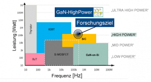
GaN (gallium nitride) is a wide-bandgap semiconductor that replaces silicon in the manufacture of electronic transistors, allowing the production of more robust components with improved operating characteristics. It is considered an emerging semiconductor on the market.
The growing interest in new semiconductor devices has led to the search for new materials such as GaN and also Sic (silicon carbide) as candidates for the construction of transistors for applications in converters for renewable energy, enabling high electrical efficiency and high power density due to to material properties, such as high speed, larger bandgap and good dynamic response.
The greater mobility and high electron saturation speed allow operation at a higher switching frequency. Furthermore, devices based on GaN and SiC (to the detriment of traditional silicon) support higher breakdown voltages and junction temperatures around twice those of silicon, enabling the reduction of component dimensions and increased inverter power density. In short, GaN and SiC allow the construction of smaller, more powerful, faster and more efficient inverters.
“In this project, the use of the latest technologies for photovoltaic inverters will be researched and tested to enable cost and weight reduction while maintaining very high efficiency. We achieved a good result at intermediate powers and now, with the new joint research project funded by the German ministry, we want to explore the potential for equipment exceeding 100 kW, which is significantly larger than the current range of applications for transistors,” he added.
“The aim is to achieve a significantly higher power density and a significantly higher power-to-weight ratio compared to previous inverters, which will result in inverters with lower material consumption, more resource efficient and also cheaper and more efficient”, he concluded .
Infineon Technologies AG, one of the world's largest semiconductor manufacturers, is another company that is part of the project. Peter Friedrichs, Vice President of Infineon's Industrial Power Control Division, explains that for the development of the project gallium nitride (GaN)-based semiconductors are being researched for the first time for high-power applications, as required in photovoltaic inverters.
“Until now, the application of GaN technology has been limited to significantly lower power ranges. It has already been demonstrated that GaN semiconductors enable even faster switching processes compared to silicon carbide (SiC) technology and even more so compared to classical silicon (Si) components. The project aims to research the extent to which the previous limits of GaN technology can be expanded”, he explains.
Vacuum Schmelze, a leading manufacturer of magnetic alloys, is also participating in the project and complements the advantages of fast semiconductors with optimized magnetic components and current sensors, which will significantly contribute to reducing the weight and volume of the inverters.
“Successful weight and volume reduction is achieved through optimized magnetic devices (inductors), with low-permeability nanocrystalline toroidal cores, which are significantly more compact and have lower losses than conventional solutions. Another aspect is the development of closed-loop sensors with high bandwidth, which also reliably measure current in the high-frequency range of GaN semiconductors”, explains Simon Sawatzki, responsible for the development of inductive components at Vacuum Schmelze.
The company TH Köln also integrates the research and provides the project with theoretical foundations for the new magnetic components. The University Hochschule Bonn-Rhein-Sieg also participates in the project and evaluates the options available for developing the hardware, in addition to preparing the integration of new components into a prototype built in the laboratory.
References
- Recent advance and future progress of GaN power semiconductor devices used in PV module integrated converters, Óscar M. Rodríguez-Benítez, Mario Ponce-Silva, Leobardo Hernández González, Juan A. Aquí-Tapia, Abraham Claudio Sánchez, Gabriel Calzada Lara, Claudia Cortés -García, 2018
- Neue Leistungselektronik für eine sonnige Zukunft


One Response
Thank you for the exposure and treatment of this entire subject, which takes us to another level of knowledge and learning about the development of new technologies, which helped us to make our electronic and command circuits more robust and smaller, and there is also a saving not only materials and components, but also greater optimization of the use of machines and equipment, and their useful life, thank you for sharing.