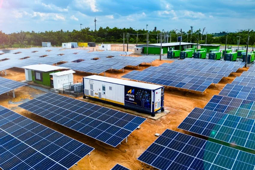
Article published in the 10th edition of Canal Solar Magazine
The manufacture of wafers, cells and photovoltaic modules follows requirements and trends relating to the raw materials and inputs used, and reducing consumption or replacing some materials may be necessary to guarantee availability, avoid environmental risks, reduce costs and increase the efficiency of the products.
The improvement or replacement of materials results in an increase in the efficiency of modules based on monocrystalline silicon (mono-Si).
P-type modules today achieve efficiencies exceeding 20%, while modules based on N-type silicon cells, in addition to heterojunction modules (HJT), provide the highest efficiencies, reaching 23% or more.
According to the International Technology Roadmap for Photovoltaic (ITRPV), the main doping element for P-type mono-Si material is gallium (Ga).
Boron (B) will continue to be replaced, as the greatest advantage of doping with gallium is the significant reduction in light-induced degradation (LID – Light Induced Degradation) of P-type material.
Light-induced lifetime degradation effects are often observed in crystalline silicon used in solar cell production.
One of the most prominent is LID, caused by the electron-induced activation of the combination between boron and oxygen in P-type cells, a phenomenon that occurs with greater intensity at the beginning of the use of the photovoltaic module.