Recently, some new types of photovoltaic cells have appeared on the market. You may have already heard about the new cell-based solar modules PERC, HJT or HIT that major manufacturers proudly announce as their latest releases.
HIT and HJT technologies
HJT and HIT are different names for the same thing. The HIT technique was developed about 20 years ago by the Japanese company Sanyo. The patent's expiration in 2010 opened a window of opportunity for other manufacturers to turn their attention to the technique.
HIT means Heterojunction Intrinsic-layer Technology and it is still a registered trademark of Panasonic (which acquired Sanyo), although the patent has already fallen.
Generally speaking, the industry refers to the technique as HJT (HeteroJunction Technology). It has already been proven possible to obtain HIT photovoltaic cells with efficiencies of more than 25% on a laboratory scale. On a commercial scale, with HIT it is possible to manufacture modules of 60 cells with powers of almost 310 W.
For comparison, with conventional technology (non-passivated silicon measuring 300 to 400 micrometers) the 60-cell modules do not exceed the 270 W barrier. Even with the reduction in cell thickness, the HIT technique increases the efficiency of the modules by up to 15% .
The HIT technique consists of adding layers of intrinsic amorphous silicon (pure silicon, without impurities or dopants) and layers of doped amorphous silicon on both surfaces of the cell.
Amorphous silicon is a type of non-crystalline silicon. It is originally used in the manufacture of thin-film solar cells, a technology that competes with (but lags far behind) mono- and polycrystalline cells.
In this case, the deposition of amorphous silicon, which occurs through a process called PECVD (Plasma-Enhanced Chemical Vapor Deposition), is only used for the passivation of crystalline silicon.
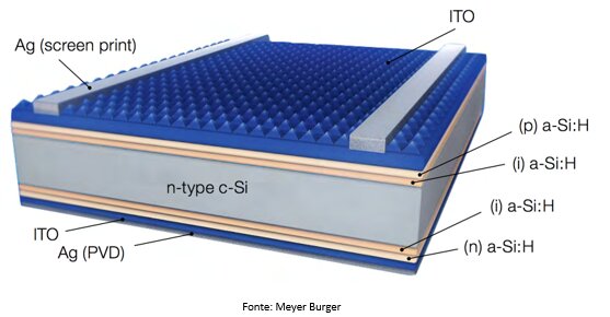
The following figure illustrates the typical structure of a HIT cell. At the bottom of the cell there is a layer of silver (Ag) metallization, manufactured by the PVD deposition process (Physical Vapor Deposition).
Continuing from bottom to top, we see that above the metallic layer there is a layer of ITO (indium tin oxide), a transparent material and a good electrical conductor. Next, we see a thin layer of amorphous silicon (a-Si) of type (n) overlaid by a thin layer of amorphous silicon (a-Si) intrinsic (i).
Next, we find a thick layer of crystalline silicon (c-Si) of type (n), superimposed by two other layers of amorphous silicon (a-Si) intrinsic (i) and amorphous silicon (a-Si) of type (p ). Finally, on the surface of the cell, there is a new conductive layer of ITO associated with metallic tracks (bus bars) silver (Ag).
This structure corresponds to the state of the art technology provided by Meyer Burguer, an important company in the technology and equipment segment for the manufacture of photovoltaic cells and modules.
Not necessarily every HIT cell has this same structure, but they all have a common principle. The principle of HIT technology lies in the existence of at least one layer of crystalline silicon (p) covered on each side by two thin layers of intrinsic amorphous silicon (i), in addition to layers of silicon (p) and (n).
The intrinsic silicon layers (i) are responsible for the passivation of type (n) crystalline silicon, while the silicon layers (p) and (n) add functionality to the cell.
The (p) layer creates an emitter on the upper surface (equivalent to the pn junction, necessary to create the photovoltaic effect) and the (n) layer creates an additional passivation surface, which gives rise to a rear electric field known as BSF (Back Surface Field), which also helps reduce electron recombination, increasing cell efficiency.
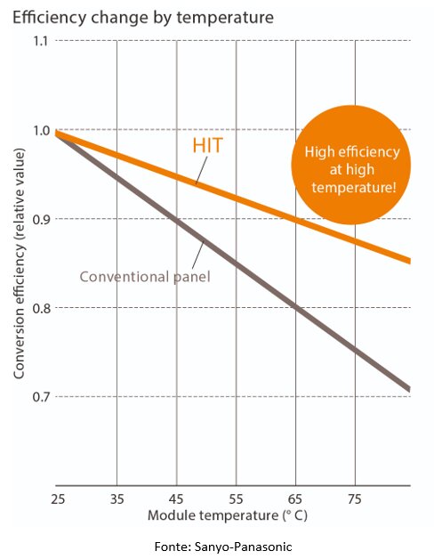
In addition to the already mentioned advantages of the HIT structure, we can also mention the reduction in the cell temperature coefficient, as illustrated in the following figure. A lower thermal coefficient (in the order of -0.26%/oC) means that the efficiency of the photovoltaic module is less influenced by the increase in temperature.
In other words, HIT modules produce more energy in hot locations than modules that employ conventional crystalline cells.
Commercial HIT modules
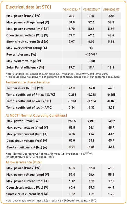
Manufacturers such as Seraphim and Panasonic make HIT modules available on the international market with efficiencies that exceed 19%. Below are the technical characteristics of the Panasonic HIT family modules.

 References
 References
- Photovoltaic Module HIT®: Converting Sunlight into Electricity with the World's Highest Conversion Efficiency
- Surface Recombination Velocity of Local Al-contacts of PERC Solar Cells Determined from LBIC Measurements and 2D Simulation, Energy Procedia, Volume 92, 2016, p. 82-87
- Surface Passivation of Crystalline Silicon Solar Cells – A Review, PROGRESS IN PHOTOVOLTAICS] RESEARCH AND APPLICATIONS, Volume 8, 2000, p. 473-487
- Advances in surface passivation of c-Si solar cells, Materials for Renewable and Sustainable Energy, 12/2012
- Electric Field Effect Surface Passivation for Silicon Solar Cells, Solid State Phenomena, 205-206, 346, Proceedings of XV GADEST
- Stable Field Effect Surface Passivation of n-type Cz Silicon, Energy Procedia, Volume 38, 2013, p. 816–822
- Momentum builds for HJT, PV Magazine, 09/2017
- Panel predictions 2018, PV Magazine, 11/2017
- Study on PID resistance of HIT PV modules, Photovoltaic Module Reliability Workshop NREL, 2013
- Heterojunction cell technology of Meyer Burger: Production processes and measuring methods, Matthias Seidel, Roth & Rau AG, Hohenstein-Ernstthal, Germany, & Rajesh Ambigapathy, Pasan SA, Neuchâtel, Switzerland
- HETEROJUNCTION TECHNOLOGY THE SOLAR CELL OF THE FUTURE, G. Roters, J. Krause, S. Leu, A. Richter, B. Strahm, Meyer Burger
- Solar Cells and Arrays: Principles, Analysis, and Design, Abdelhalim Zekry, Ahmed Shaker, Marwa Salem
- Panasonic HIT Heterojunction technology
- PERC cell technology explained
- The Passivated Emitter and Rear Cell (PERC): From conception to mass production, Solar Energy Materials and Solar Cells, Volume 143, 2015, p. 190-197