
In the photovoltaic solar energy market there are basically two families of technologies: crystalline silicon and thin films.
Crystalline technology, to which mono and polycrystalline silicon belongs, is responsible for the largest market share and accounts for almost all photovoltaic cells and modules manufactured in the world.
On the other hand, there is an interesting niche market for the technology called thin films. The manufacturing process for thin films is diametrically opposite to that of crystalline semiconductors.
While in crystalline technology cells are manufactured from sawdust of solid silicon ingots, cells and thin film modules are manufactured from the deposition of small semiconductor particles on surfaces that can be rigid or flexible.
The thin film deposition technique is employed in many areas of industry and is an important field of study in materials science.
Thin film deposition is the act of applying a thin layer of a material to the surface of another material, modifying the physical or chemical characteristics of the receiving material.
The process of deposition of a thin film can be carried out by several methods, among which one of the most used is physical vapor deposition (PVD – physical vapor deposition).
The PVD technique corresponds to the deposition of a material on a surface through its vaporization inside a heated vacuum chamber.
The material to be deposited is vaporized by applying a high temperature. Deposition can occur through a purely physical process or can involve chemical reactions on the surface of the substrate (material that receives the thin film).
The result of physical vapor deposition is the production of a thin film, more commonly known as a thin film, of the material that has been vaporized.
The vaporization speed can be controlled, allowing layer thickness to be adjusted. It is also possible to subject the substrate to several deposition stages, gradually adding several layers of the same or different materials.
Advantages of the thin film deposition technique
The manufacture of thin films using the vapor deposition process uses controlled quantities of materials, avoiding waste, and is more energy efficient than the manufacture of crystalline silicon.
In the manufacture of mono or poly crystalline ingots, high temperatures are required to fuse the silicon, which requires large amounts of energy.
The process then requires sawing the silicon to manufacture wafers, a process in which losses occur. Furthermore, manufacturing thin films is faster and requires fewer steps than manufacturing crystalline cells.
The myth of low efficiency of thin films
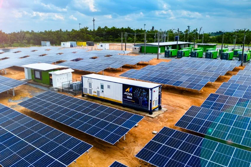
Thin-film photovoltaic devices occupy a very small share of the power generation market, but the benefits and promises surrounding this technology stimulate much effort in the research and development of thin-film photovoltaic cells and modules.
A known disadvantage of the thin film photovoltaic cell is its reduced efficiency compared to crystalline silicon.
This is true when it comes to thin films of amorphous silicon or even microcrystalline silicon, which require the production of cells with two or more junctions (the manufacturing process of which is more expensive) to obtain cells that can compete in efficiency with silicon. crystalline.
Several research centers and manufacturers around the world have been looking for new materials for the manufacture of thin films with a good cost-benefit ratio.
Outstanding among these materials are cadmium telluride (CdTe) and copper-indium-gallium-selenium alloy (CIGS), which allow the manufacture of photovoltaic cells and modules with efficiencies that reach (and may even exceed) the marks achieved by crystalline silicon devices.
CIGS photovoltaic cells
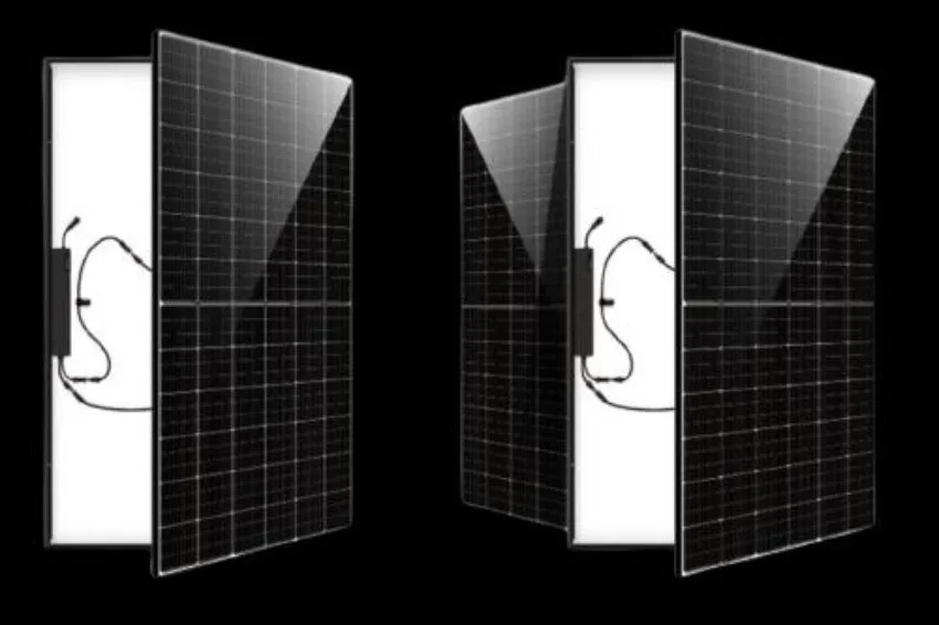
CIGS (copper-indium-gallium-selenium) is one of the main materials currently used in the manufacture of thin film photovoltaic cells.
CIGS has a good sunlight absorption coefficient, allowing the use of thinner layers than would be required with other types of semiconductors.
CIGS cells have already been manufactured in laboratories with efficiencies greater than 21% and commercially the modules have efficiencies ranging between approximately 15% and 18%, very close to the efficiencies of crystalline silicon modules.
CIGS is one of the only materials technologies, alongside CdTE, that can commercially compete with crystalline silicon.
While the large power generation market massively uses crystalline silicon, there are several applications in which CIGS cells stand out.
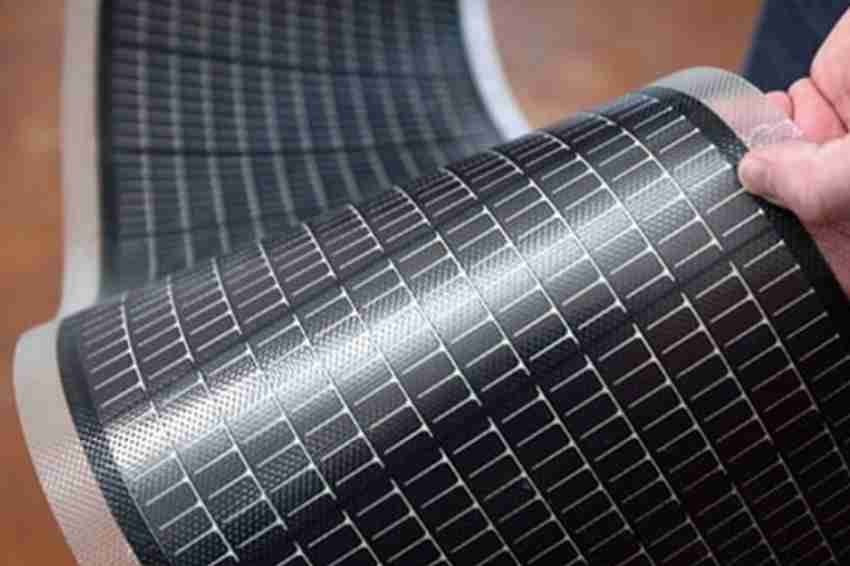
CIGS films can be deposited on plastic or glass surfaces, allowing the creation of a variety of photovoltaic products, such as flexible modules and tiles with different formats.
 is applied. After a very thin N semiconductor layer, a final conductive and transparent layer of zinc oxide with aluminum is applied, responsible for the front contacts of the cell. Source: TU Delft")

, cadmium sulfide (N material), and zinc oxide (transparent conductor for the front contacts)")
Despite all the advantages presented, there is a major problem in the scalability of the production of CIGS cells and modules: element “I”, indium, is one of the rarest materials on the planet.
The graph below gives us an idea of how difficult it is to find Indians in nature. However, indium is also used in the manufacture of electronic components and displays, so its commercial availability is not negligible.


Why CIGS?
When the objective is to produce flexible photovoltaic cells and modules or those with non-planar shapes, the only possible option is the use of thin films.
Crystalline silicon cells are necessarily flat, rigid and very brittle, requiring robust and heavy structures, with glass and an aluminum frame, for their packaging.
Flexible photovoltaic modules, roof tiles, awnings, vehicle covers and decorative elements for building facades can be produced from thin films. Crystalline silicon is not an option in these cases.
Among the material options for the production of thin film photovoltaic devices, CIGS is one of the best alternatives, as already mentioned in the previous section.
The table below shows a comparison of the efficiency of photovoltaic modules produced with the main commercially available technologies.
For better comparison, the following table only refers to the efficiency of rigid photovoltaic modules with glass.
Although thin films have always been touted as an alternative for non-conventional photovoltaic modules, CIGS technology also competes in the rigid photovoltaic module market.
Table 1: Efficiencies of PV modules with different technologies. Source: Introduction to Photovoltaic Solar Energy Course (UNICAMP)")
")
Some advantages of CIGS modules
- Sustainable production, with the use of fewer energy resources and a smaller volume of raw materials. A CIGS cell is 100 times thinner than a crystalline silicon cell;
- Reduced thermal coefficient. This is an advantage found in all thin films, which suffer less from temperature rises;
- Thin film modules are good absorbers of diffused light and are suitable for installation in a vertical position, which allows them to be integrated into architecture. They can be used as cladding on building facades and installed in locations that are typically not suitable for the use of crystalline modules;
- They can be manufactured in small or large dimensions, without the size restrictions known in crystalline modules due to the fragility of the cells;
- They do not suffer from the problem of microcracks like crystalline modules;
- CIGS modules come close to the efficiency of commercial crystalline modules, with the advantages of thin films.

Table 2: Mechanical and electrical characteristics of a commercial CIGS module with an efficiency of approximately 14.58% (calculated from specifications). Source: NICE Solar Energy, Germany
. Source: NICE Solar Energy, Germany")
CIGS photovoltaic tiles
Photovoltaic tiles are some of the countless application possibilities for CIGS thin films. In addition to allowing the manufacture of tiles in different formats (curved, flat, wavy), CIGS technology is far superior to crystalline in this particular type of application.
There have already been attempts to produce photovoltaic tiles in the industry using crystalline silicon cells, but the results of these attempts are only tiles with photovoltaic cells on top – and not genuinely photovoltaic tiles.
In addition to not allowing coverage of the total area of the tile with photovoltaic material and greatly limiting the formats and dimensions of possible tiles, crystalline cells are not suitable for this type of application due to their fragility, their high thermal coefficient and their vulnerability to shadows.
Thin film cells are manufactured in very small widths, which makes it easy to produce tiles with voltages from several tens to a hundred volts.
On the other hand, photovoltaic tiles with crystalline cells will naturally present low output voltages (due to the small number of cells used), which makes it necessary to connect a large number of tiles in series in practical applications.
Photovoltaic tiles with crystalline cells still suffer from other problems such as the cells being subject to microcracks, the low number of cells per tile (which makes the product inefficient) and the impossibility of covering the entire roof area with photovoltaic material (which also This results in low system efficiency.
Finally, a problem often overlooked by manufacturers of photovoltaic tiles: the shape of the tile causes shadows on its own cell, which substantially reduces efficiency in practical applications – as if all the other problems found in this type of product were not enough.

Photovoltaic tiles made from CIGS films are an excellent solution from a technical and aesthetic point of view.
In addition to their uniform appearance, CIGS films enable high efficiency and allow the entire roof area to be covered by photovoltaic material, maximizing the use of the area available for installation.


One Response
Good afternoon Marcelo,
I would like to do a pilot with the film based on CIGS films. I say Pilot, installation in buildings, several apartments with the aim of reducing the thermal load and still generating energy. Can we talk about it?